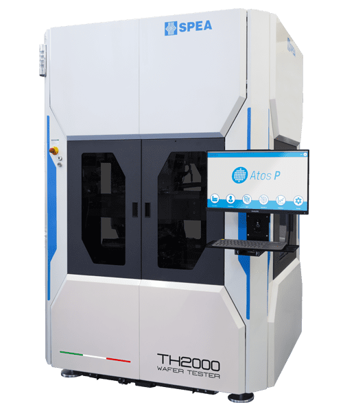
TH2000 is a revolutionary automatic wafer prober which combines double-sided wafer probing capability with comprehensive test resources, including electrical test, HV/HI test, warpage and surface verification, and optical inspection.
The system performs complete, high-throughput tests at wafer level for the most challenging applications, including power devices, optoelectronics, pass-through dies, multi-project wafers, complex systems-on-a-chip and unconventional layouts, with size up to 12” (300mm).
The probing technology based on multiple flying probe cards and the lean test process (all the tests required at wafer level are performed in a single step) make TH2000 able to dramatically lower your cost of test.
Fully automatic double-sided wafer prober
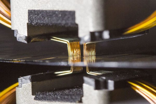
Simultaneous double-sided probing and testing
Eight independent axes provide parallel test capabilities, which shorten the overall process time (indexing + test time). Each probe can test a dedicated area of the media in parallel with the others, while a single die can be simultaneously contacted from top and bottom.
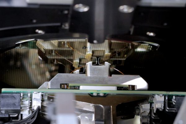
Planarity and position compensation
Actual Z-heights are profiled and automatically compensated by each axis, in order to overcome any planarity issue. The exact positioning over the wafer surface is monitored and compensated by roto translation of the wafer, so to adjust as needed.
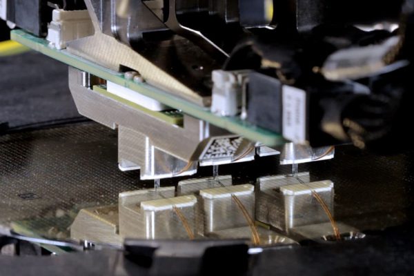
Fast and precise probing
Hi-Speed Linear Motors with Hi-Resolution Linear Optical Encoders are used on each XYZ axis, to ensure high throughput and best probing accuracy. The system chassis made of natural granite provides high stiffness, excellent vibration damping, thermal stability, to avoid any loss in accuracy due to movement speed and environmental variations.
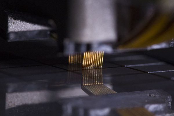
Gentle contacting
Ultra Soft Touch technology allows TH2000 to contact the most delicate and smallest dies without leaving marks, thanks to a programmable overdrive (down to 1 gram) and controlled motion profiles.
Flying Multi Probe Cards
TH2000 brings the versatility of flying probe technology to semiconductor manufacturers. Each TH2000 axis can be equipped with a single-site or a multi-site probe card with different die shape or pitch, including unconventional and high-density geometries. The possibility to have different probe cards on the different axes make TH2000 suitable to test also multi-project wafers.
The probe cards can be based on different technologies (cantilever, spring probes, MEMS probes, wiring probes), and can be designed according to every die density/shape/map: testability issues are no longer a limit to your wafer layout, that can be designed in order to minimize the cost per die.
Built-in complete test capabilities
Multi-Function Flying Head
TH2000 axes can be equipped with single or multi-die probe cards, laser meter, high-resolution vision units, to perform all the tests required. Electrical tests include analog, digital, mixed signal, high-voltage and high-current tests. The most accurate measurements can be performed, thanks to the fact that a mini DUT-board with signal conditioning resources can be placed directly on the system flying axes, to be as close as possible to the DUT. The possibility to probe the same pad on both sides simultaneously makes it possible to perform accurate measurements with no influence from the adjacent pads.
Mechanical tests include planarity, height and warpage tests.
Optical inspection is able to detect scratches, lithography and pattern defects, particle presence, cracks and imperfections.
Lean Test Process
All the tests required at wafer level are performed in a single step, with the same probing machine, with no need for additional testers or inspection stations. You can take the advantage of reduced test equipment footprint, higher throughput, lower test costs. TH2000 can accept manual product loading, or it can work in a test cell in pass-back mode, with the integration of an automatic loader.
