Volpiano (Italy)
July 04, 2022
The new 3.2Gbps test module at Semicon West 2022
SPEA announces the company will preview, at the next-coming Semicon West in San Francisco, a new 3.2Gbps card option for its DOT800 test platform. The new digital channel module puts the DOT800 at the forefront of the digital transformation, addressing key technologies like wireless broadband communications, high-performance computing, medical imaging, artificial intelligence, consumer audio and video, automotive connectivity. The tester is now able to offer the highest cost-efficiency covering the test requirements of next-generation SerDes, DAC/ADC converters, buffer/level translators, DVI/HDMI interfaces, SoC and microcontrollers.
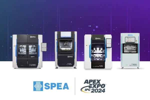
At booth #1929 located in South Hall, SPEA will also demonstrate its wide range of semiconductor test equipment, including power semiconductor testers, analog mixed-signal testers, MEMS test cells and wafer probers.
New High-Speed Digital Channel Module
Featuring up to 128 digital channels on a single instrument, the new channel option enables the DOT800 to perform high multi-site, cost-efficient testing of high-speed communication interface devices, which require a spread spectrum modulation on channels and clock signals to verify their signal integrity and robustness against EMI.
Designed with per-pin DSP and a comprehensive DSP library for digital data calculation, the module reduces the test time and simplifies the pin/channel assignment, speeding up the load board development. Protocol aware architecture contributes to efficiently implementing DUT communication on a wide variety of standard protocols, reducing pattern complexity and test program execution time, while simplifying the debug and characterization process.
Flexible waveform generation, low-jitter high-speed clock signals with jitter modulation, and timing flexibility, are the perfect fit for testing high-speed applications.
In combination with the other modules of the LPE series, this new card option further empowers the device-oriented instrumentation that is at the heart of DOT800’s technology.
Device Oriented Tester: Your Tester, in a Board
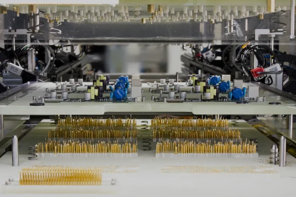
The successful DOT800 will be on display at SPEA’s booth in San Francisco. This innovative analog mixed signal tester is based on a revolutionary tester-in-a-board concept: All the resources required to test one – or multiple – devices are housed on a single board, allowing you to greatly simplify the load board connections between tester channels and device.
This multi-processor, multi-function channel instrument combines analog, digital and signal processing capabilities, including multiple control CPUs, DSP modules and programmable logic units. The LPE board is modular and configurable: It can be composed with an on-board controller, and up to four channel cards that can be selected to build the perfect performance mix to satisfy the customer’s test requirements, for a total of up to 256 channels in a single instrument slot. Each individual channel card features a dedicated matrix card, simplifying the design of the load board and reducing the quantity of relays installed. The tester can be populated with one-type instruments, greatly simplifying system composition, programming and maintenance, while satisfying at best all the device test requirements.
Advanced predictive maintenance activities are automatically carried out by the tester: DOT800 collects, analyses and notifies any deviation from standard performances, in order to take the required actions and avoid process degradations and system downtime. All the instruments have an on-board memory used to evaluate their mechanical wear, while the tester autonomously verifies the instrument calibration data (with no need to remove the load board) and, when performances are out of specs, automatically launches the instrument calibration procedure.
The solutions for power semiconductor testing
With its DOT800T, SPEA provides a complete solution for Power testing, combining on a single machine all the resources to perform ISO, AC, DC test on the whole range of power applications. This tester is expressly designed to address the test requirements of traditional Silicon devices as well as new Gallium Nitride and Silicon Carbide technologies, covering their performance range with the highest voltage and current source capabilities, high frequency and low current measurement capabilities. A multi-core architecture allows DOT800T to perform accurate static, dynamic and isolation tests on dedicated stations, each of which with a dedicated independent controller. The different test programs are performed in a true parallel, asynchronous mode, since each test core controller manages test resources, instrument connections, and test program execution.
Expanding MEMS Test Capabilities
SPEA, with its recognized industry-leading test cells for MEMS devices, combines in a single equipment all the elements of handling, contacting, physical stimulus and complete testing and calibration of MEMS and other IC devices, at ambient or temperature conditions.
On the H3580 handler platform, multiple stimuli can be housed in a single test unit, to test combo MEMS, such as environmental sensors (pressure + humidity + gas + temperature) or navigation sensors (accelerometer + gyroscope + compass). Throughput capabilities are over 33,000 units per hour, offering the possibility to test as many as 396 devices simultaneously.
The flexible and modular architecture facilitates an easy in-field reconfiguration of the test area, replacing MEMS stimulus units and test modules.
In San Francisco, SPEA’s MEMS test technology will be represented by the highly successful inertial test unit for testing low g accelerometers and gyroscopes, by accurately stimulating with precise and reliable angular position, rate and acceleration motion.
The new double-sided wafer prober and tester
TH2000 is a revolutionary system which combines double-sided wafer probing capability with comprehensive test resources, including electrical test, HV/HI test, warpage and surface verification, and optical inspection.
The system performs complete, high-throughput tests at wafer level for the most challenging applications, including power devices, optoelectronics, pass-through dies, multi-project wafers, complex systems-on-a-chip and unconventional layouts, with size up to 12” (300mm).
The probing technology based on multiple, flying probe cards, and the lean test process (all the tests required at wafer level are performed in a single step) make TH2000 able to dramatically lower your cost of test.
Beyond the Exhibition: Technical Presentation about ATE modeling in application development
In addition to its exhibits, SPEA will sponsor and participate in the Test Vision Symposium on July 13-14. During the second session on July 14, Luca Fanelli, Business Development Manager of SPEA’s Semiconductor Test Division, will talk about how “ATE Instrument Modeling Speeds Up Time To Market and Load Board Design’‘. The speech will explore how the inclusion of the ATE Instruments models, as part of the signal chain to DUT, will reduce debug time and costs while at the same time extending the efficacy of traditional simulations like PDN Impedance analysis, Signal Integrity analysis, Insertion Loss Simulations and many others.