Turin (Italy)

January 23, 2024

In-Circuit testing: detecting electronic board defects

in circuit testing


What is In-Circuit testing and which are its advantages


In-circuit testing is a common test method, used in high-volume manufacturing environments, that verifies the performance and the integrity of electronic printed circuit boards before they leave the production floor.
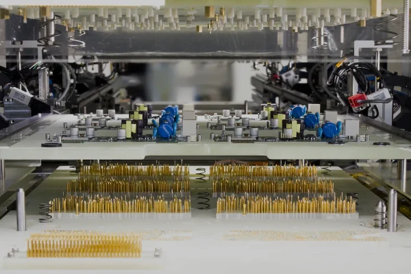
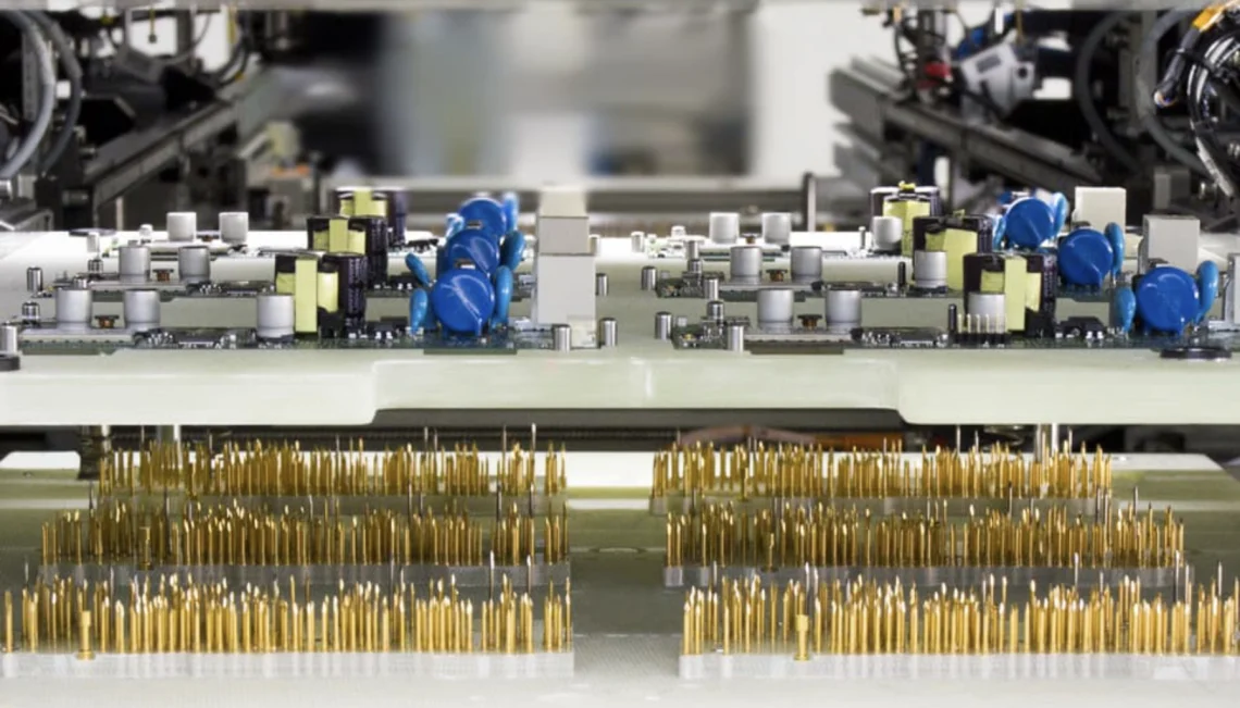
 Through probes making electrical connections with the PCB test points, ICT test detects any possible electrical defect either on the board or in the installing components.

Implementing In-Circuit Testing (ICT) significantly boosts the overall production efficiency of PCBA manufacturing. ICT test is highly precise at catching manufacturing flaws. It can find shorts, where electrical paths are unintentionally connected, and opens, where connections are broken.

It can also detect wrong or missing components. This makes in-circuit testing a powerful tool that helps reduce missed defects, giving manufacturers confidence that the electronic boards will work properly.

Since its introduction, the in-circuit test has marked a significant advancement over conventional functional test methods, profoundly transforming the landscape of printed circuit board assembly (PCBA) validation.

This evolution has substantially elevated the quality of test coverage, as direct access to every net on the board provides unparalleled diagnostic precision, a capability unmatched by functional testing alone. In fact, PCBAs that successfully undergo ICT are more likely to operate properly, resulting in enhanced product reliability, greater customer satisfaction, a stronger brand image, and reduced warranty claims.


How does ICT testing work


The ICT testing process starts with setting up the in-circuit tester. ICT test equipment suppliers utilize extensive CAD analysis and probe placement techniques to evaluate circuit board designs.
After defining the test method and program, the PCBA is positioned within the test area. The in-circuit tester then sends electrical signals to assess various parameters. This comprehensive evaluation includes:

  • Basic electrical functionality
  • Component values and characteristics such as resistance, capacitance, ICs digital and analog functionality
  • Assembly defects like shorts or open circuits, wrong, missing or misoriented components

Following these measurements, the tester rigorously compares the collected data against predefined specifications. Any detected discrepancies lead to the in-circuit tester marking the PCBA for either rework or rejection.

Every in-circuit test generates data that can be used to improve the manufacturing process. Trends or recurrent issues can be identified at an early stage and can be addressed before they become expensive problems. Integrating this data with manufacturing systems, such as MES software, is crucial for optimizing workflows. This integration ultimately leads to enhanced quality, reduced downtime, and more streamlined production processes.


How is ICT test performed on PCBAs


ICT test on PCBAs can be performed through various testing methods. Manufacturing Defect Analyzer (MDA) stands as a valuable guardian in PCBA production.

Although MDAs identify the majority of manufacturing defects at an early stage, they lack the capability to conduct powered tests or assess the behavior of active components, rendering them inadequate for complete circuit validation.

This is where bed-of-nails testers and flying probe testers come into play, ensuring comprehensive in-circuit testing coverage.

Bed-of-nails testers and flying probe testers can be both used for in-circuit testing to ensure the quality and functionality of printed circuit board assemblies (PCBAs).

  • Bed-of-nails testers feature many tiny spring-loaded pins arranged to contact test points.
  • Flying probe testers move over the PCBA making contact at the different locations of the test points without a fixed fixture.

As they differ significantly in their approach and application suitability, the choice between these in-circuit test methods depends on specific production needs regarding volume scale and design complexity.

Typically, bed-of-nails in-circuit testers better handle fast and high-volume manufacturing scenarios requiring greater accuracy and shorter test time without compromising production rates and costs.

SPEA automatic in-circuit testers meet this demand successfully by harmonizing high-volume ICT testing and low costs with the requirements of accuracy and short test time. This is also expressed in the guidelines for the SPEA bed-of-nails ICT testers.

Ranging from manual boards loading to fully automated in-line testers, the SPEA bed-of-nails in-circuit testers ensure comprehensive defect detection at the highest throughput.


Which testing capabilities optimize In-Circuit testers


SPEA bed-of-nails in-circuit testers are designed to address the rigorous demands of modern high-volume manufacturing, offering a combination of features that deliver exceptional performance:

  • High test parallelism. The ICT testers’ architecture is based on a multi-site test area design and independent cores, which facilitate the parallel testing of boards or panels of boards, achieving speeds that can be up to ten times quicker than traditional approaches. This feature permits the simultaneous in-circuit testing of multiple boards or different models
  • Versatile testing. SPEA bed-of-nails ICT testers run a real-time variety of testing techniques including ICT, digital and analog functional testing, flashing, and power testing, all integrated seamlessly into the production line. This reduces the need for multiple testers to handle high-volume productions, cutting investments in both maintenance and industrial space.
  • Superior accuracy in defect detection. Beyond speed, SPEA bed-of-nails testers for in-circuit testing are a step ahead in early defect detection thanks to their extreme measurement accuracy and advanced parameterization algorithms. The SPEA DeepICT™ testing technology identifies weak components that would later cause malfunctions in the field, thereby preventing costly product returns and significant business losses.
  • Designed for autonomy. SPEA in-circuit testers ensure production continuity with minimal operator intervention. Flexible automatic modes, including robot integration and automatic board loaders/unloaders, eliminate manual operations. Embedded smart sensors constantly monitor performance, optimize usage, and predict maintenance needs, greatly reducing the risk of testing interruptions and delays.


Key Takeaways on In-Circuit Test


In-circuit testing remains a key player in electronic manufacturing. Its ability to quickly detect faults and ensure product quality makes ICT test invaluable.

By leveraging advanced techniques, from the foundational MDA to sophisticated bed-of-nails and flying probe in-circuit testers, ICT ensures that PCB Assemblies are meticulously verified for shorts, opens, and component anomalies.

The advancements in ICT, particularly exemplified by SPEA high-speed, multi-site, and extreme accuracy, not only streamline the test process but also provide fundamental data for continuous manufacturing improvement.


Watch the video about In-Circuit Testing


FAQs

In-circuit testing (ICT) is a test method that verifies the integrity of every single component on an assembled electronic board. Using a bed-of-nails fixture to contact test points on the board, SPEA’s ICT testers measure resistance, capacitance, and inductance, and verify component presence and orientation, as well as identifying shorts and opens. This approach, often performed before full board power-up, detects manufacturing defects very early in the process, ensuring the build quality and reliability SPEA has been known for since 1976.

The main purpose of ICT testing is to ensure the assembly quality of electronic boards by identifying manufacturing defects as early as possible in the process. This allows to:

  • Detect structural defects like shorts, opens, missing, incorrect, or faulty components.
  • Increase production yield by catching faults before they become more expensive to repair.
  • Reduce overall testing and repair costs.
  • Ensure high reliability of the final product, a cornerstone of the SPEA philosophy.

The fundamental difference lies in the objective and the level of verification:

  • In-circuit testing (ICT) focuses on the board’s structure and its components. It verifies that each component is present, correct, and properly oriented, and that electrical connections (no shorts or opens) match the schematic, regardless of the board’s final function.
  • Functional testing (FCT) evaluates the overall behavior of the board or module. It simulates real operating conditions to verify that the device performs the functions it was designed for.
    SPEA provides both ICT bed-of-nails testers and flying probe testers, often combined on a single platform, to ensure both assembly correctness and final product performance.

Both are ICT test methods for electronic boards, but they differ in how they contact the board:

  • ICT bed-of-nails tester uses a fixed piece of equipment called “fixture”. This jig, specific to each board type, contains hundreds or thousands of pins that simultaneously contact all test points. It is extremely fast, making it ideal for high-volume production.
  • Flying probe tester uses no fixture. It employs a number of probes (typically 4 to 8) that move rapidly across the board, contacting test points sequentially. It is very flexible, perfect for boards with high density or no dedicated test points.
    SPEA offers both technologies, with its flying probe systems known for speed and precision, and its ICT bed-of-nail testers for efficiency in mass production.
Share with

Download Our In-Circuit Testing Brochure


    Thank you!

    We just sent you an email with the required documentation

    Design & Code by dsweb.lab